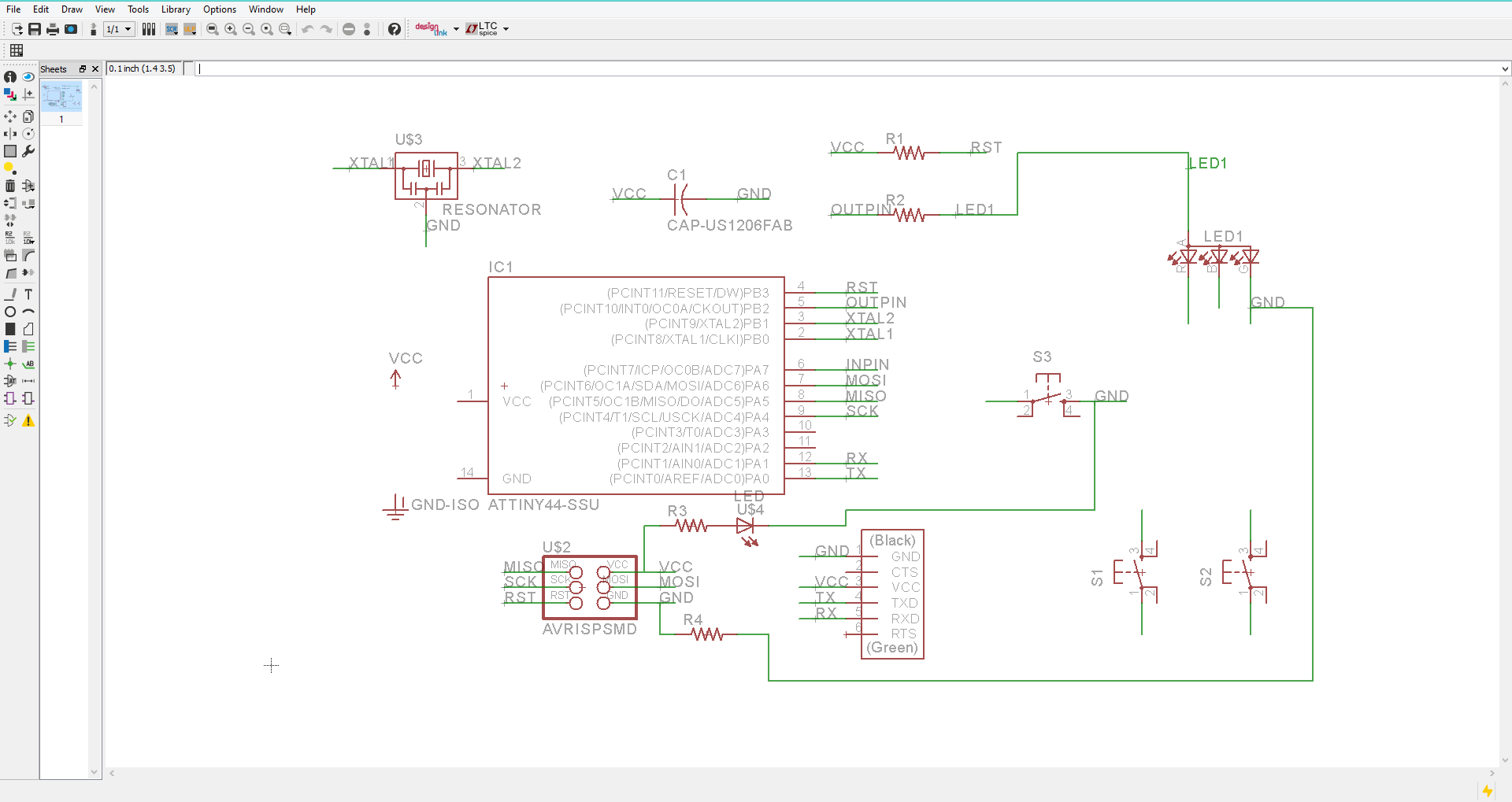
This week I designed a development board of sorts based around the Attiny44. It has 3 buttons an on/off status led and one RGB led. This project was pretty straight forward since I have used Eagle before. In Eagle you incorperate electronic componenets into your schematic through libraries of componenets. Many places like Adafruit and Sparkfun have component libraries available for download. I already had the Fab Lab component library downloaded so I got to skip that step. Then using the add component tool I placed my components and linked the connections between then using the naming tool instead of drawing wires between them all. This makes your schematic look much cleaner. All in all Eagle is a great software for circuit and circuit board design but sometimes finding the part you are looking for can be a huge pain. |
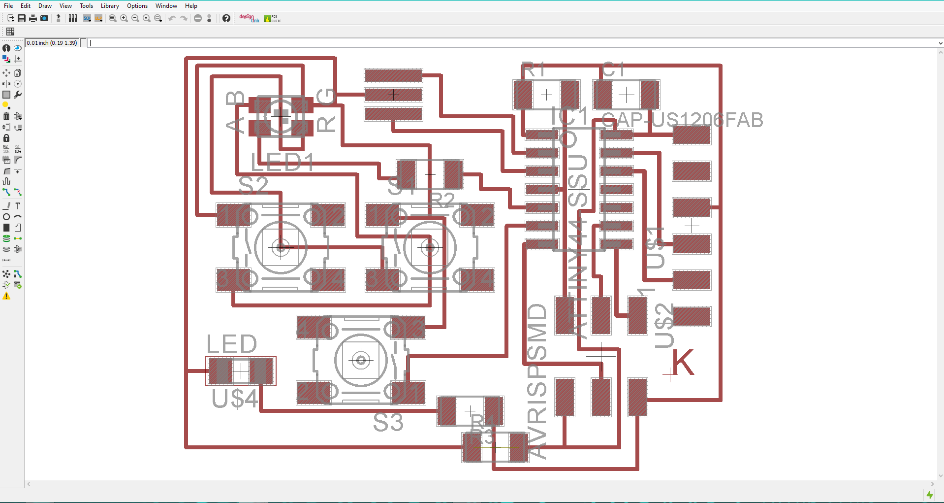
Once I designed my circuit I went on to design the board layout for my circuit. In Eagle this is a pretty straight forward process, but when making a single layer board it can be tricky to make all of your traces neat. Using 0 ohm resistors as jumpers to jump over other traces is a life saving trick. In Eagle all of your components will show up in board view and little yellow lines will connect the components together. Using the traces tool you can draw the connections in the way you would like until you cannot see anymore yellow lines. At this point as long as your circuit is correct you are done designing your circuit board in Eagle. One note, my line thickness was set at 0.016. This turned out to be rather thin and though it did work the traces are fragile. |
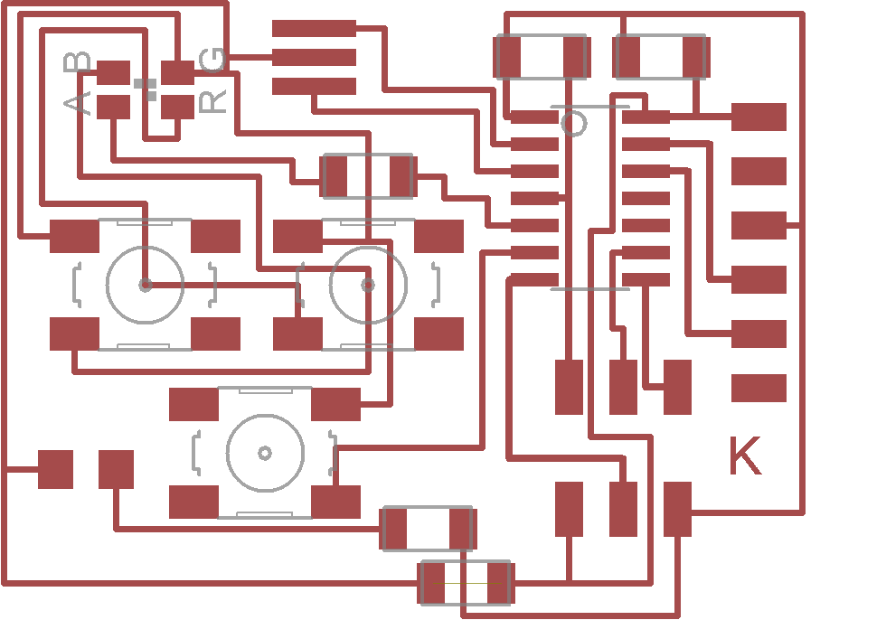
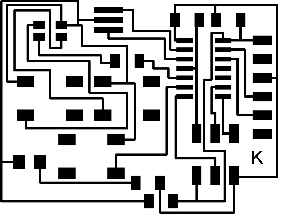
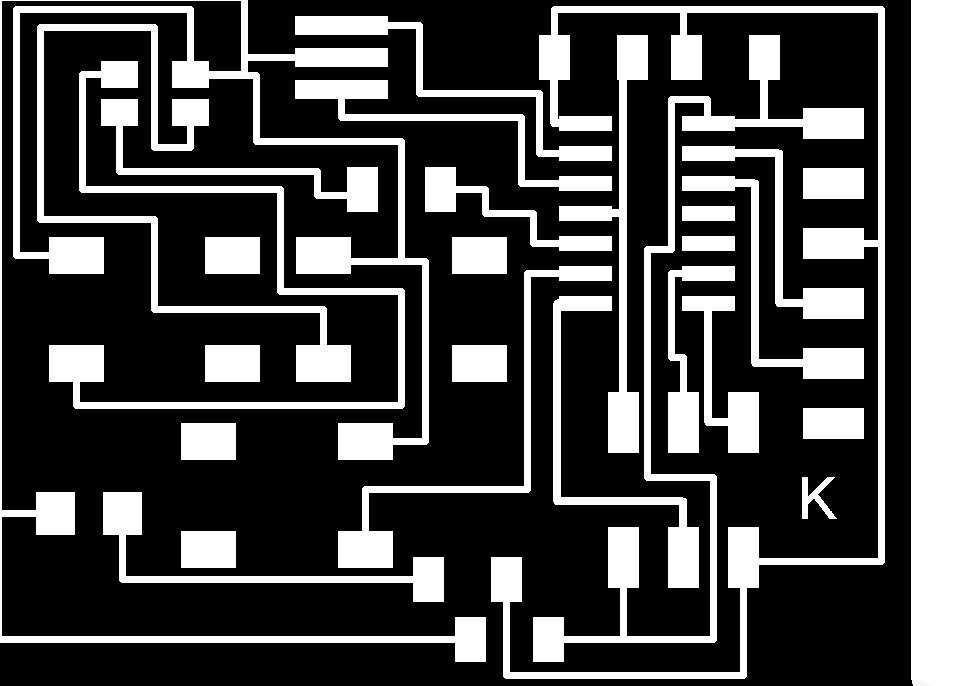
Once my board was done all I needed to do was disable all of the layers except for my traces. This can be done by going to the layers menu in Eagle. I think exported the traces in monochrome. I opened the saved file in Gimp and inverted the colors so the traces and pads were white and the area I wanted to remove was black. |

The next step was simple but very important. I duplicated the file containing the traces, opened it in Adobe Illustrator and drew a rectangle around it. Then I deleted the traces so all that was left was the outline of my board, remember to make sure that the line thickness is at least 1/32 so the mini mill will cut it. |
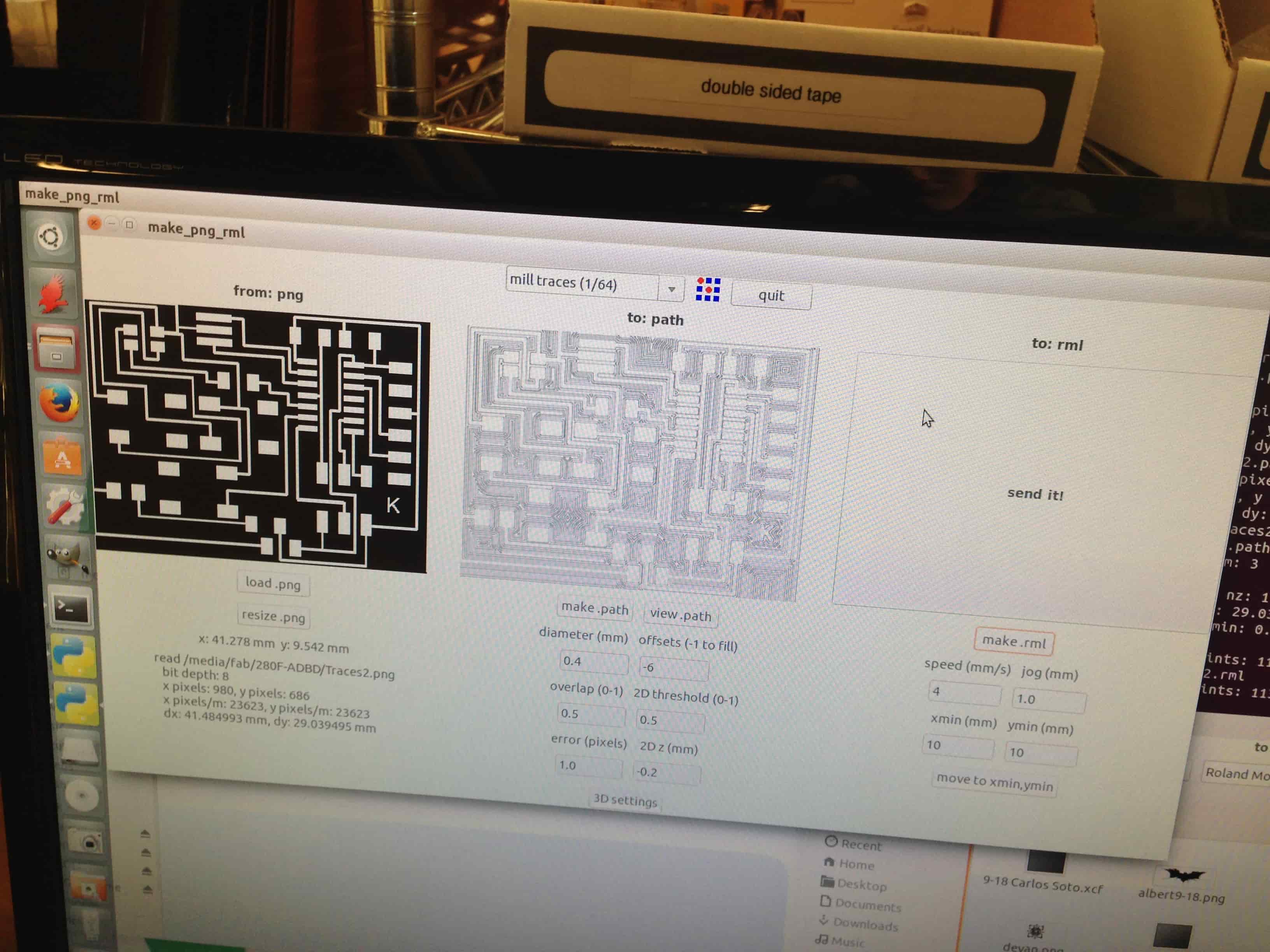
After all my design work was finished I opened the traces in the Fab Module and set the settings to default except for the fill which I set to -6. Then I hit "send it" and the cut started. See my earlier Fab ISP for a more detailed explanation of using the Modela Mini Mill to cut circuit boards. |
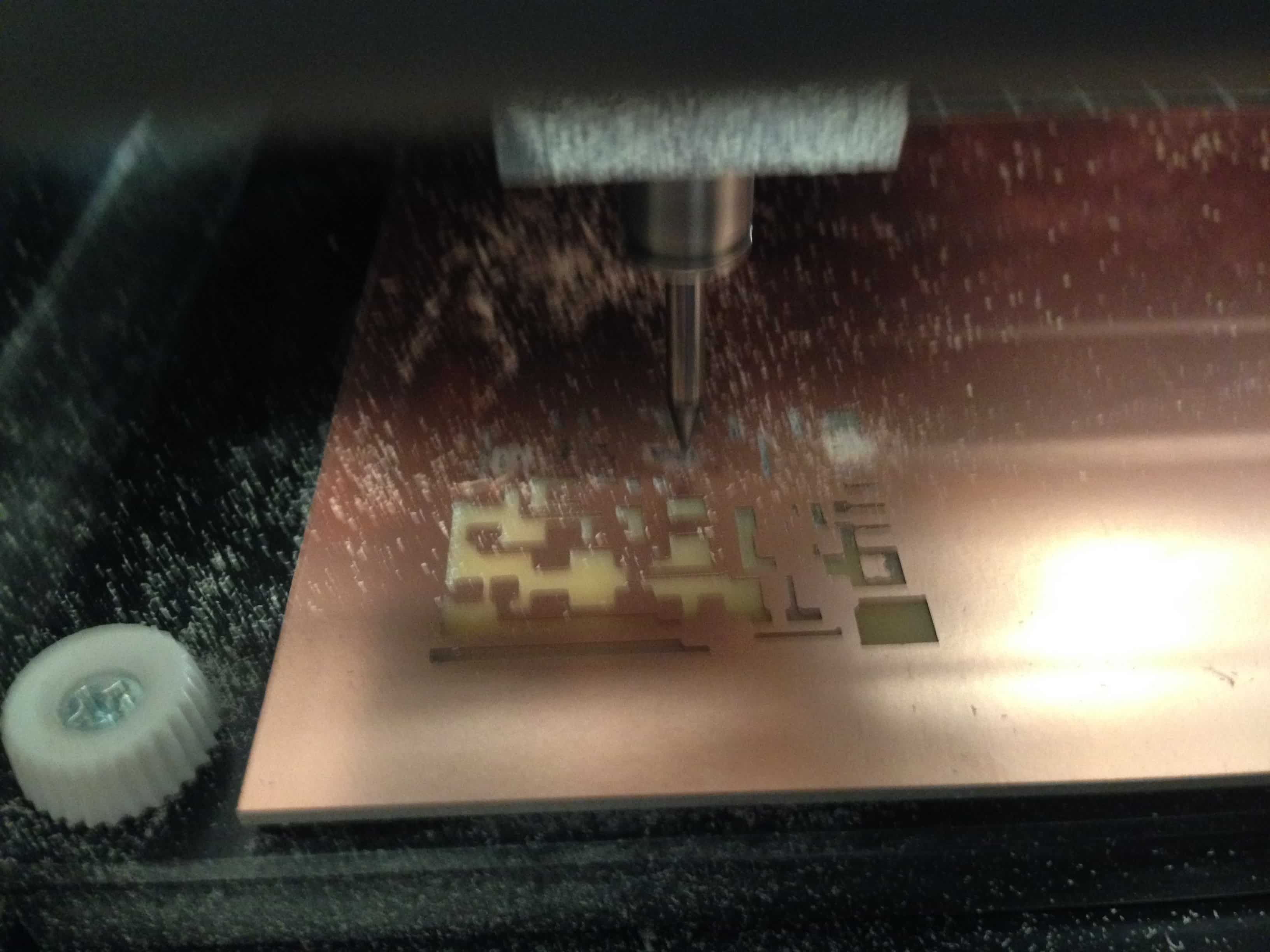
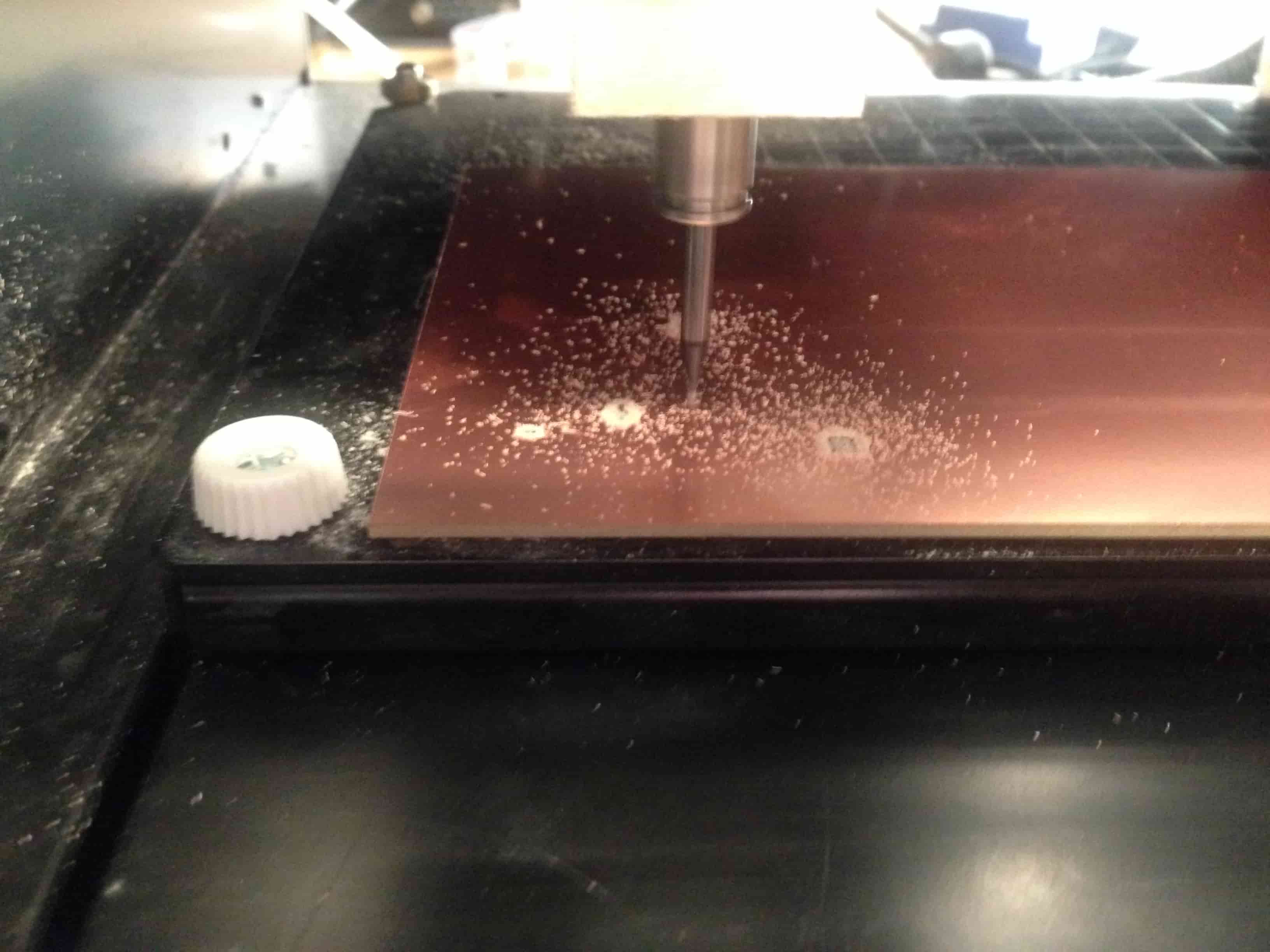
The board took about 15 minutes to mill out. Then I switched to a 1/32 bit and loaded my outline file, again using the defaults for the 1/32 bit. |
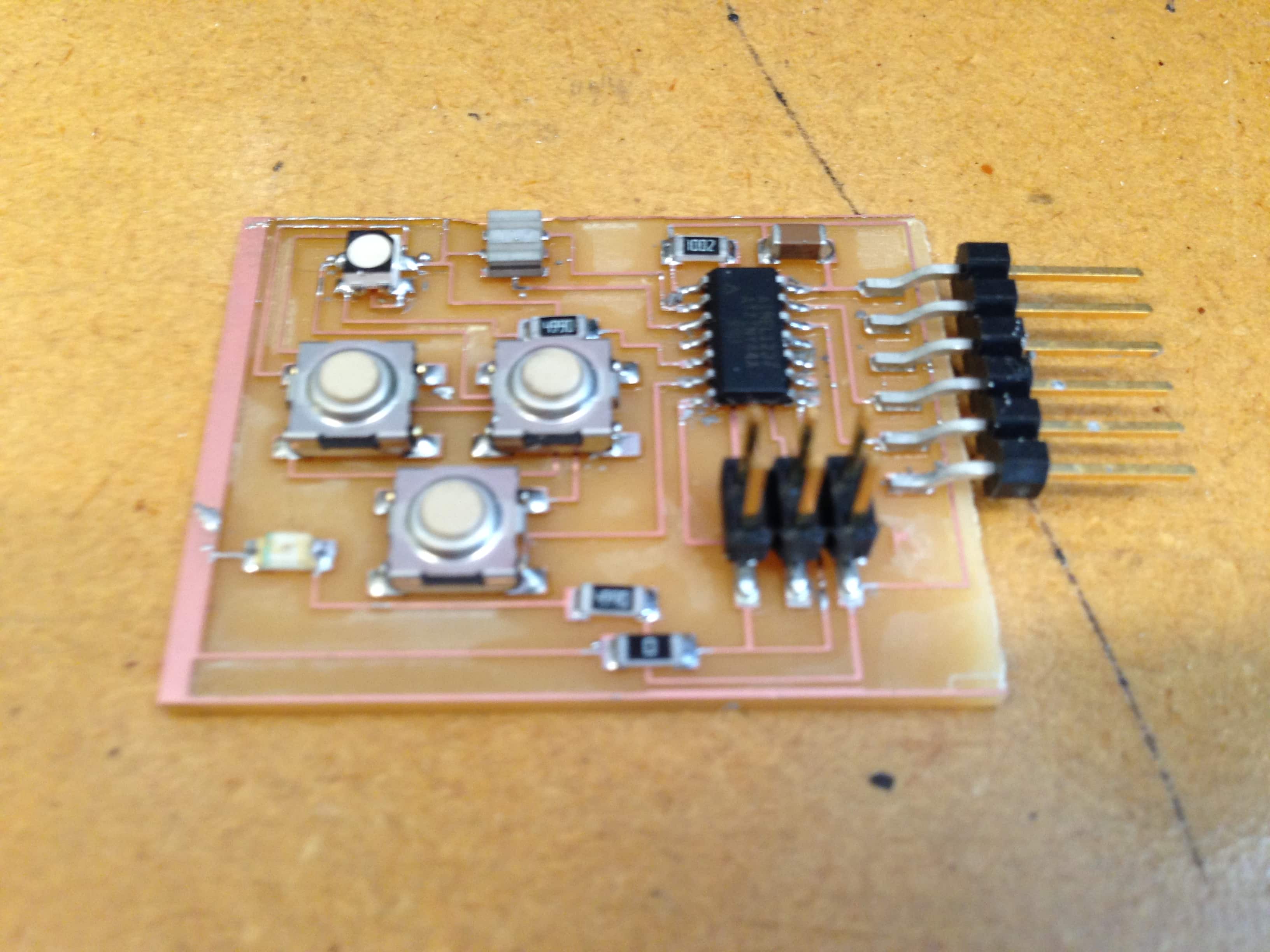
Once the board was completely milled out I used tweezers to apply solder paste to the pads where components would be placed. Then I placed the SMT components and used a hot air reflow gun set to 270 degrees to melt and solidify the solder paste. Make sure when using a reflow gun with surface mount components to keep the airflow very low so you do not blow your components out of allignment. |

But when your done don't forget the Fablab tradition of Fabbercise. I decided to take it to the next level with some outdoor moutain biking adventures here in Anchorage, Alaska for my weekly dose of fabbercise. |